
Your detector doesn’t just collect data— it defines its limits.
How does electron microscopy data from hybrid pixel detectors compare to monolithic active pixel detectors, what are some examples that people can buy, how does it impact the data quality, what are the limitations imposed by the detectors, what accelerating voltage are they optimized for?
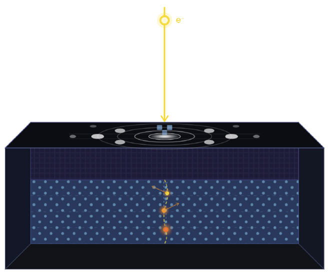
BACKGROUND: Hybrid pixel detectors were developed originally as x-ray detectors but have found success in electron microscopes as well. Their cost-competitiveness has made them attractive options as much of the R&D is driven by global initiatives and international collaborations. Many of the design decisions, however, are driven by X-Ray interactions rather than electron interactions. This drives some of the fundamental decisions such as pixel and sensor size as well methods for counting. Examples of repurposed x-ray hybrid pixel detectors include the Medipix (Merlin), Timepix(Cheetah), Arina, Stella, Singla, and EMPAD cameras.
On the other hand, Monolithic active pixel sensors (MAPS) were developed originally for electrons with the DE-12 as the first commercial product kicking of the “Resolution Revolution”. The small pixel size integrated and counting modes are all designed with the higher interaction volume of electrons in comparison to X-rays. Examples include Celeritas, Celeritas XS, DE-16, K2 and K3.
Speed in 4D-STEM detectors depends on readout circuitry, silicon design, and bit-depth limitations. Most detectors have a slower framerate when reading the entire sensor, but they can achieve higher speeds by using binning, smaller readout areas or reducing bit-depth. It is important to understand how many pixels and how many electrons-per-pixel are needed to analyze the feature of interest in your 4D-STEM. Then detector settings can be chosen that will determine the framerate of the experiment. The important metric for a microscopist choosing a camera is ”4D-STEM patterns-per-second”, rather than the maximum “frames-per-second”. So how do the different camera specifications affect the maximum “4D-STEM patterns-per-second’’?
Hybrid detectors use large pixels (55-150 µm) to try to stop electrons fully in the sensitive layer. This limits the number of pixels that can fit on a sensor. So, hybrid detectors are typically limited to a maximum of 256 x 256 pixels. Any hybrid detectors larger than this are typically squeezing 4 smaller sensors alongside one another, resulting in a cross-shaped dead area on the camera.
MAPS detectors use small pixels (5-15 µm) that let electrons pass through them. They typically have 1024 x 1024 pixels or more with no dead area. This is an important consideration if you want to use the camera for TEM diffraction, Micro-ED, TEM imaging or if you anticipate your 4D-STEM pattern having many small spots that need to be identified for strain mapping. Having many pixels is also advantageous for performing precise pattern-shift corrections.
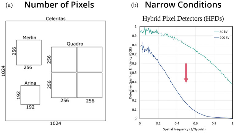
Figure 1: (a) A comparison of the 1k x 1k Celeritas sensor to different hybrid pixel detectors. (b) Detector quantum efficiency (DQE) plots for a Medipix 3 hybrid detector at 80kV and 200kV. The performance drops drastically due to charge spreading to adjacent pixels at 200/300 kV.
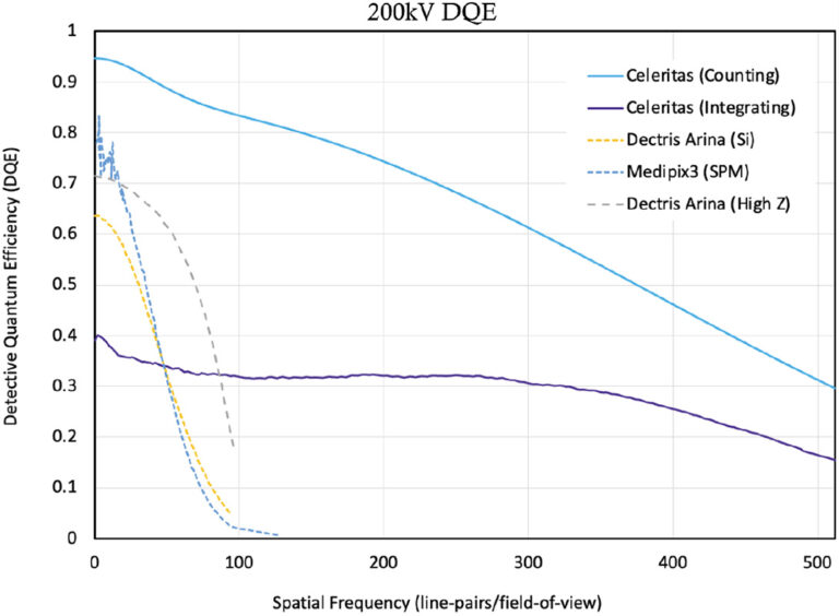
Figure 2: DQE curves for the Arina and Medipix 3 hybrid detector compared to a MAPS detector (Celeritas)1,2. Having much fewer pixels, the efficiency of hybrid detectors drops rapidly for medium-sized features and they cannot properly resolve small features such a diffraction disk-edges.
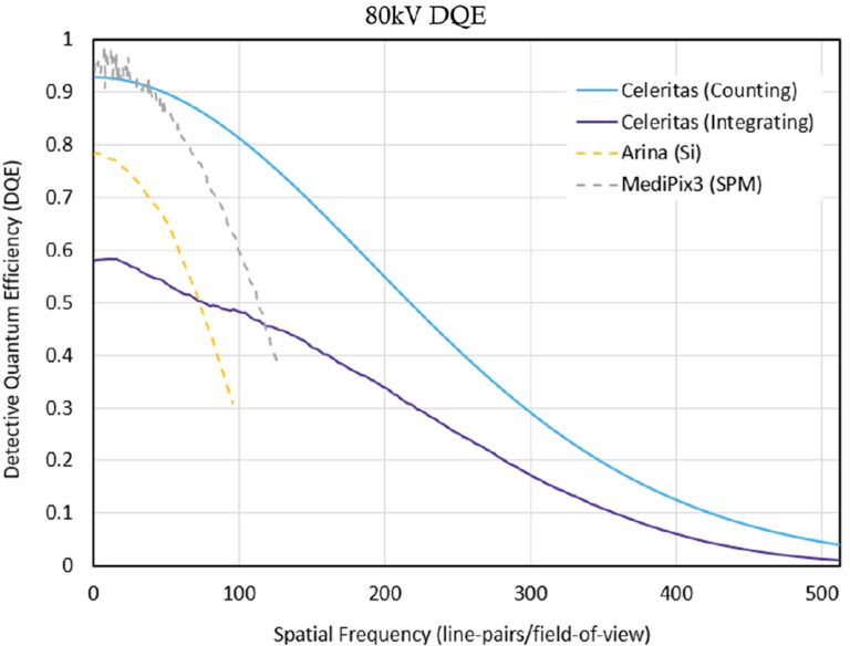
Figure 3: DQE comparison at 80kV for the Arina and Medipix hybrid detectors compared to the MAPS Celeritas1,2. The hybrid detectors’ DQE(0) is higher than for 200kV, but again drops rapidly, showing poorer performance for medium-sized diffraction features and an inability to resolve small features.
Detector Quantum Efficiency (DQE) measures how efficient a detector is at resolving features of different sizes. The resolving efficiency for larger objects such a bright field diffraction spot with a large convergence angle is shown on the left of the graph. For the detector manufacturers (and the savvy user) this also gives important information about the proper detector pixel size and (if you should be binning). At 200 keV for the Medipix and Si Dectris Arina, almost no information is left at high frequencies, meaning that almost no information is lost by binning the data by 2. This also means that the pixels are undersized for higher keV. The higher Z sensor is more effective at capturing the frequency information at the cost of worse semi-conducting performance.
The efficiency then gradually decreases for medium-sized features such as smaller diffraction spots (middle of the graph). Towards the right of the graph is the efficiency for imaging of small features such as the edge of diffraction disks. Figure 1(b) shows how the quantum efficiency of hybrid detectors drops drastically from 80kV to 200kV. This is a consequence of the 200kV electrons having more energy to deposit, which blurs the signal from one electron across multiple pixels. As the energy deposited increases as the electron slows, most of the energy is deposited farther away from the entry point. This is the main consequence when using hybrid detectors with pixels designed for X-rays rather than TEM electrons.
By contrast, the DQE of MAPS detectors increases between 80kV and 200kV. This is because the electron passes through the sensor, and at 200kV it deposits less energy, making it less likely for one electron to produce signal in multiple pixels.
But how does the DQE compare between the two types of detectors? This is shown in Figure 2 & Figure 3. For context, direct detectors can operate in two different modes; counting /single pixel mode (SPM) is more sensitive but requires a low beam current on the camera, whereas integrating/charge summing mode is less sensitive but can handle more beam current.
The hybrid detector starts with a reasonable DQE of ~0.8 in SPM, but has much fewer pixels so the resolving power drops rapidly and it cannot resolve small features in middle or right of the graph at all.
For the Celeritas MAPS sensor, counting mode DQE is ~0.95 at 200kV for large objects and remain good for all frequencies/feature sizes. Integrating mode begins with a lower DQE for larger objects, but it retains a relatively good DQE even for the smallest features on the detector. In short, MAPS sensors offer far better performance for resolving complete 4D-STEM diffraction patterns, while hybrid detectors perform well when only the bright field disk needs to be recorded.
Dynamic range is often quoted but also often misunderstood. It is commonly expressed in terms of electrons/pixel/second, but also be expressed in terms of electrons/pixel/frame or electrons/second on the camera. These all depend on the readout area, binning, and the pixel depth for different cameras. A microscopist should be careful to check that the dynamic range quoted is valid for the maximum frames per second or readout area desired.
Hybrid pixel detectors achieve dynamic range by using charge summing mode (CSM), MAPS detectors use integrating/linear mode. Both approaches involve dividing the total signal collected in a pixel by the average signal deposited for one electron.
Comparing the maximum number for the hybrid Medipix/Merlin detector (16.7×10⁶) to the MAPS Celeritas XS (7×10⁶) detector in terms of electron/pixel/second, hybrid detectors have ~2.5x the dynamic range of the fastest MAPS detector.
While prices vary by company and camera model, there are some general guidelines that can be observed. Hybrid pixel detectors using re-purposed x-ray sensor technology will typically be available for a lower price owing to the lack of research and development costs.
MAPS detectors are all custom designed for electrons, and thus are generally more expensive, but entry-level MAPS detectors compete at a similar price to hybrid detectors. The highest performance MAPS detectors are around 2x the price of hybrid detectors.
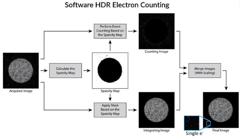
MAPS detectors from Direct Electron have the advantage of using HDR counting. This separates the image, then applies integrating mode to areas with high signal, and counting mode to areas with weak signal. This approach gives counting mode DQE to the dark-field and so it enhances the signal-to-noise ratio of weak diffraction spots around 2.5 times.
Hybrid detectors are unable to combine SPM and CSM mode, so they cannot implement the same approach.
CONCLUSION:
MAPS and hybrid direct detectors offer distinct tradeoffs. It is important for electron microscopists to understand the advantages and limitations of each detector and assess how well the detector suits their planned experimental techniques.
In general hybrid detectors at 80kV offer good 4D-STEM imaging of the intense bright field disk for a lower price. However, they will struggle to pick up weaker diffraction spots and smaller features will appear blurry, especially if used at 200 or 300kV.
MAPS detectors are better suited to 200/300kV, and offer higher performance when recording full diffraction patterns and attempting to perform precise measurements or alignments of the 4D-STEM data. MAPS detectors also off more flexibility in terms of the large range of techniques that the detector can be used for, but they generally cost more than hybrid detectors.
References:
