
For a low-kV direct detector for TEM, see our DE-16ER: Extended Voltage Range page.
With the goal of propelling electron microscopy to new frontiers, Direct Electron introduced the first large-format Direct Detection Device (DDD®) in 2008, as the culmination of academic and industrial partnerships working through many generations of sensor development beginning in 2001. As the pioneer in direct electron detection, our revolutionary DDD sensors were recognized with the 2010 Microscopy Today Innovation Award.
Based on our flagship DE-Series cameras for electron microscopy, we have extended direct detection technology for low voltage electron microscopy. Just as biological cryo-EM was revolutionized several years ago by direct detectors, low voltage EM techniques (such as LEEM/PEEM) are now on the cusp of a similar revolution. Achieve results you never before thought possible at low voltages with incredible images and data collection at incredibly high speeds. We’ve created a camera that gives you dramatically better resolution and a larger field-of-view, with full-frame unbinned streaming at up to 92 frames per second (fps) for motion correction or analysis of dynamics. Our product allows for direct detection of 10 – 40 keV primary electrons—a revolutionary advancement in data quality. With 8x more information per image compared to MCP + CCD, our technology yields stunning images every single time.
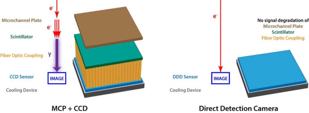
Traditional low-energy electron detectors use a microchannel plate (MCP) to multiply the incident primary electrons. The resulting cloud of electrons from the MCP then travels to a phosphor scintillator which converts these electrons to photons, which can be detected by the CCD imaging sensor. Resolution is degraded in several of these steps, including the electron multiplication in the MCP, the conversion to photons in the scintillator, and the transfer from the scintillator to the CCD detector.
In contrast, our DDD directly detects image-forming electrons in the microscope without the use of a MCP or a scintillator. The result is dramatically better resolution, signal-to-noise ratio, and sensitivity.
The secret to the DDD’s high performance is its radiation hardened sensing layer. Incident beam electrons enter this thin layer, leaving an ionization trail that is collected and integrated to form a signal. Electron counting can be performed on the data to further improve signal to noise and resolution. Image distortions are minimized since the DDD directly detects electrons without having to transfer signal through fiber-optic or optical lenses.
A second innovative feature of the DDD is its high frame rate, with no dead time between frames. This high frame rate delivers intrinsic dose fractionation during image acquisition, which can be exploited for motion correction, damage compensation, and other image processing techniques. High frame rate data acquisition also enables challenging applications such as in situ TEM.
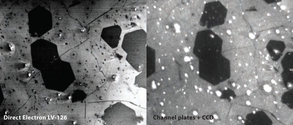
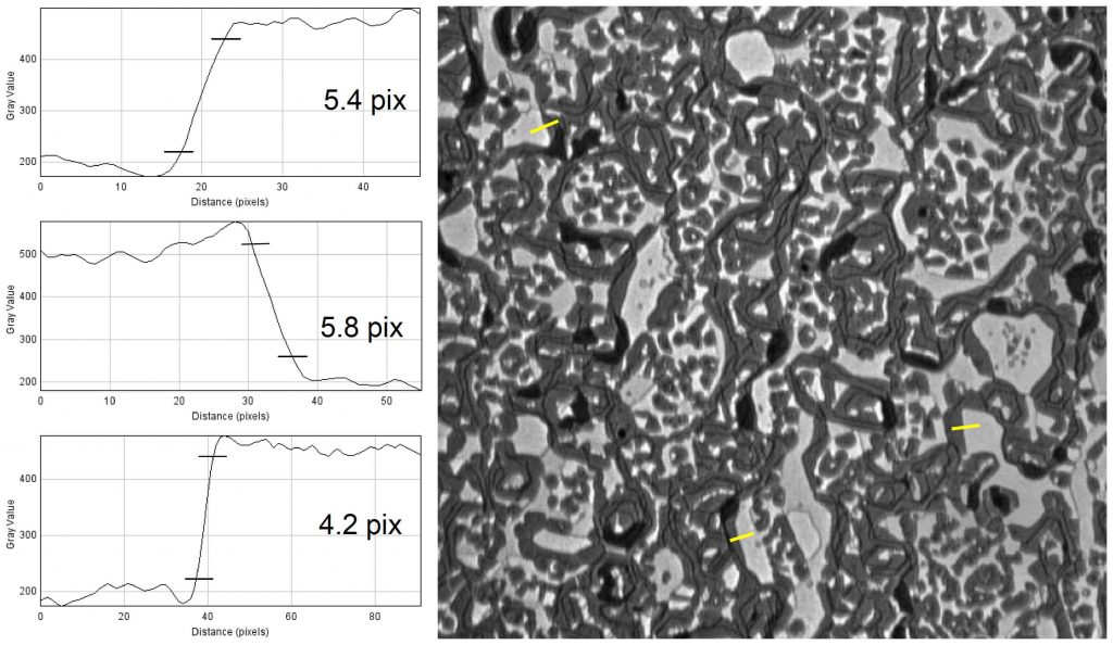
Our first prototype low-kV detector was known as the LV-126. Compared to conventional detectors for low-voltage EM (microchannel plates + CCD), the LV-126 delivered significantly better resolution. This boost in resolution not only significantly improved image quality, but it also allowed users to collect images at lower magnification in order to dramatically increase the field-of-view. Indeed, at constant resolution, the LV-126 delivered approximately 8x more information than a conventional low-voltage EM detector. Our new LV-16 detector offers an even larger field of view, faster imaging speeds, and larger pixels for improved resolution.
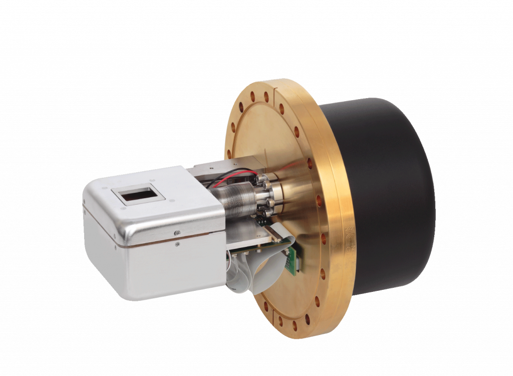
With high sensitivity and excellent resolution, the LV-16 offers exceptional performance for 10-40 kV applications.
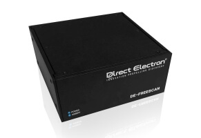
As an accessory to the LV-16, the DE-FreeScan adds capability to scanning mode experiments.
