
Meridian is a new EBSD camera based on the prototype DE-SEMCam installed at UC Santa Barbara. In testing, this 4096 x 4096 sensor provided the highest-resolution EBSD patterns ever recorded, enabling high-angular-resolution (HR)-EBSD analysis for strain mapping, dislocation density mapping, low-voltage orientation mapping of beam-sensitive ceramics, and energy-filtering of patterns from 3-30keV. Meridian uses the same sensor, typically operating in bin2 mode to produce 2048 x 2048 pixel patterns at 281 pps. While it can also be used for standard orientation mapping, Meridian excels at HR-EBSD applications where the important crystallographic characteristics appear as subtle changes in the EBSD pattern.
In a major change from the prototype SEMCam, Meridian features a miniaturized camera head, placing the sensor in the traditional EBSD orientation. This combined with the 26.6mm sensor width allows Meridian to collect a large solid angle of backscattered electrons. When higher spatial resolution is needed, Meridian can tilt automatically to TKD (Transmission Kikuchi Diffraction) orientation without breaking vacuum.
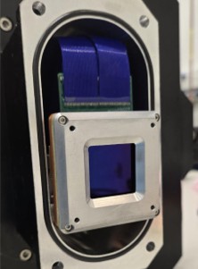
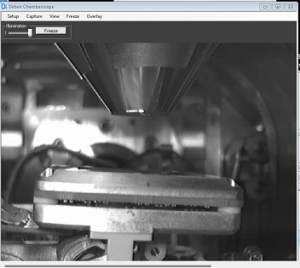
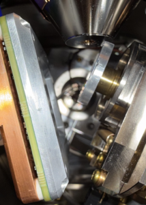
Meridian EBSD detector installed at the National Institute of Standards and Technology (NIST)
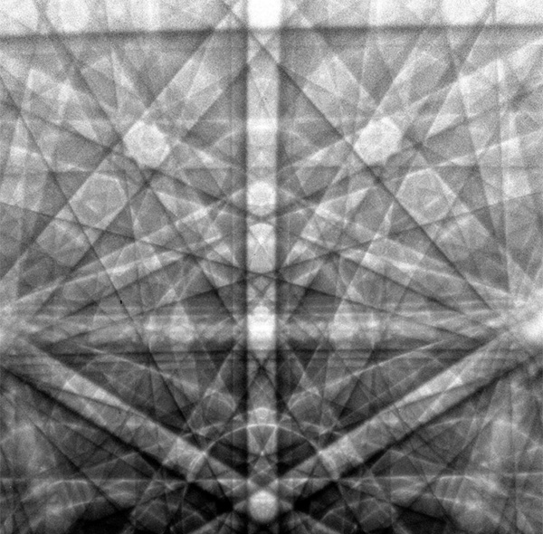
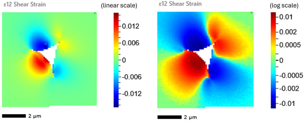
HR-EBSD 12kV pattern and strain maps of a silicon indent
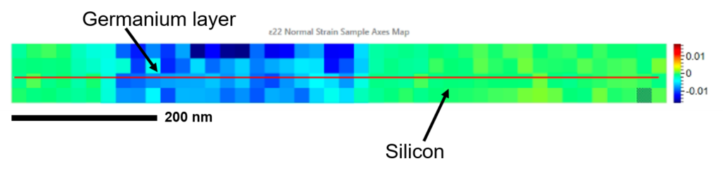
HR-EBSD analysis on Meridian enables strain mapping to a precision of 0.01% . The analysis is facilitated by the CrossCourt software package from BLGVantage. Meridian’s monolithic active pixel (MAPS) sensor provides a high DQE at high frequencies. Compared to a hybrid-pixel direct detector, or a traditional scintillator-coupled camera, Meridian records the band edges with high contrast from fewer scattered electrons. Thus the collection time for HR-EBSD is much faster than with alternative detectors. Importantly, Meridian can operate with high sensitivity down to 3keV. Since interaction volume is reduced, the spatial resolution at 5kV is 20x smaller than at 30kV. Thus Meridian can provide strain mapping with <20nm spatial resolution.
Some materials, such as ceramics present challenges for routine EBSD data collection and indexing due to small grain sizes, high crack densities, beam and charge sensitivities, low crystal symmetries, and pseudo-symmetric pattern variants. Micro-cracked hafnia/hafnon composites exhibit all of these challenges, but Meridian was able to successfully map these samples. For this work, indexing was performed in OIM analysis, and EMSoft (dictionary indexing). We are happy to announce that Meridian will soon be able to do its own live indexing in Direct Electron’s Mission Control software. Full details of the hafnia/hafnon work can be found in this article in Ultramicroscopy.
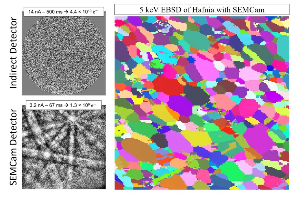
Orientation mapping of micro-cracked Hafnia at 5keV using the Meridian sensor
The strength of additively manufactured metallic materials is often governed by ~0.5µm dislocation cells. The Meridian sensor was used to collect HR-EBSD patterns with high enough quality that the pattern sharpness was used to map the density of these dislocation cells in 316L stainless steel, and two superalloys. Read the full manuscript here.
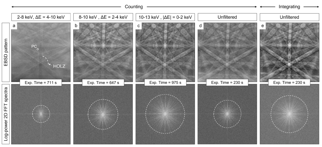
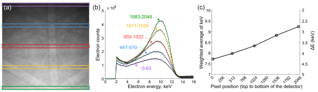
Meridian’s exceptional signal-to-noise ratio for single electrons means that the charge deposited on the sensor can be directly used to measure the energy of each electron. This has been applied to filtering HR-EBSD patterns of silicon at 12kV to increase the pattern sharpness (above). Even in integrating mode, the FFT “spokes” extend past the mid-point, representing ½ Nyquist frequency of the 2048 x 2048 pixel pattern. That means that these smallest features could not have been captured on a detector smaller than 2048 x 2048.
Meridian can also be used to record the energy spectrum from different regions of the pattern (below). Read the full details in this ultramicroscopy article.
Meridian is ready to order now.
Looking for something else? We offer a full range of products for electron microscopy:
Apollo | Celeritas | DE Cameras | LV-16 | DE Freescan | Software
If you have questions about our products, head to our FAQ page, or contact us to learn more.
