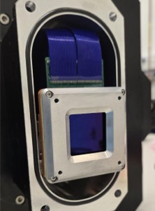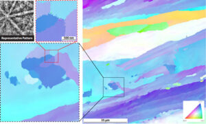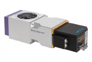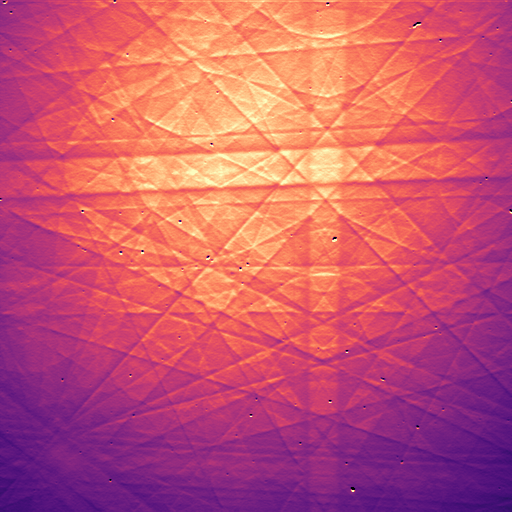
In a preprint recently posted on arXiv, researchers from the University of California at Santa Barbara have reported using a new monolithic active pixel sensor (MAPS) based direct detector designed by Direct Electron for collecting electron backscatter diffraction (EBSD) data. As has previously been demonstrated in Transmission Electron Microscopy (TEM), by eliminating the need for a scintillator and fiber-optic coupling, direct detectors can achieve a higher detective quantum efficiency and a higher signal to noise ratio than conventional detectors. This is advantageous for EBSD as well as TEM imaging.
The new MAPS based detector is optimized for voltages typically used in SEM and EBSD. With 2048 x 2048 pixels, the detector offers high resolution EBSD pattern acquisition at a rate of 281 patterns per second. Pattern acquisition speed can be increased by reading out fewer rows of the detector. These rows need not be contiguous, allowing full EBSD patterns to be sub-sampled. Acquisition speeds of almost 6000 patterns per second have been demonstrated.
The preprint can be found at this link: https://arxiv.org/abs/2008.11411